白皮書
Leveraging 3D layout to optimize PCB designs

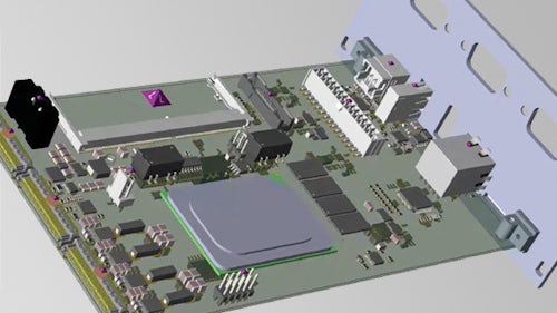
Visualize and validate PCB designs as if they were already manufactured. With Xpedition, designers and engineers can easily understand the physical product, enabling identification of electro-mechanical problems early in the design cycle and avoiding costly re-designs. A photorealistic view of all board elements also helps with flex design challenges.
6 ways to maximize the benefits of 3D PCB design
- Use 3D layout for viewing, placement, and more
- Add 3D parts quickly and easily
- Set 3D constraints and clearances
- Communicate with MCAD
- Improve flex design with advanced 3D layout
- Help manufacturers capture the design intent with 3D PDF
Learn more about 3D layout with Xpedition Enterprise.
相關資訊
White Paper
電子介面的設計生命週期
設計和驗證新一代電子系統的高速介面非常困難,而且會隨著產品、流程和組織的複雜度增加,變得更加困難。在將 DDR 用於連接處理器 / 記憶 體時,改善效能導致餘裕減小,需要建立更繁複的約束條件和拓撲,並提高整體設計的複雜度。本白皮書將重點介紹流程和組織的複雜度,以及如何處理這些問題。