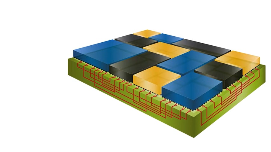
Pushing the system-in-package concept into the future
Chipletz selected Siemens semiconductor packaging technologies for the design of their unique Smart Substrate based advanced packages

Chipletz
Incorporated in 2021, Chipletz is a fabless substrate vendor developing advanced packaging technology that bridges the gap between the slowing of Moore’s Law and the rising demand for compute performance. The company’s Smart Substrate products facilitate multiple ICs in a single package for critical AI workloads, immersive consumer experiences, and high-performance computing. Chipletz is targeting delivery of its initial products to its customers and partners in early 2024.
- 本社:
- Austin, Texas, United States
- 業種:
- エレクトロニクス, 半導体デバイス
We selected Siemens as they demonstrated their technologies’ capability and capacity, along with their expertise in advanced heterogeneous semiconductor package design.
Vision
Chipletz is a funded start-up with industry veterans from Advanced Micro Devices, Inc. (AMD) and other major system providers. Their vision is to revolutionize semiconductor in-package functionality through the development of an advanced packaging technology that bridges the gap between the slowing of Moore’s Law and the rising demand for compute performance. Chipletz Smart Substrate products facilitate the heterogeneous integration of multiple ICs in a single package for critical AI workloads, immersive consumer experiences, and high-performance computing.
The Chipletz team of skilled engineers have decades of experience in semiconductor design, manufacturing, and packaging to address that need. Chipletz is pushing the system-in-package concept into the future and offering a path forward that will enable years of additional performance increases while resetting the economic model for semiconductor integration. Chipletz makes integration of virtually any die from any manufacturer possible using their unique Smart Substrate based platform.
The Smart Substrate provides die-to-die interconnect and high speed I/O and supports different voltage domains from a single supply, outperforming current multi-chip module and system-in-package options.
-640x360.jpg?auto=format,compress&w=843&q=60)
Michael Su, CTO and Bryan Black, CEO of Chipletz
“Designing for our Smart Substrate has a number of challenging requirements for designers and their design tools,” said Michael Su, CTO at Chipletz. “These were key evaluation drivers for us when we evaluated EDA suppliers and their technologies.”
The key selection criteria Chipletz used can be summarized as follows:
- Support for high bandwidth memory
(HBM) channel design - Interactive performance on very large
designs with very large connectivity
structures - Advanced substrate degassing
capabilities - Creation of complex power and ground
structures using reuse - Design tool and design flow automation
and customization - Ability to develop custom Smart
Substrate specific design rule checks
(DRC) - Supplier domain expertise and technical
resource availability and credibility
To evaluate the Siemens Xpedition™ semiconductor packaging technology, Chipletz used a design consisting of a very large SoC flanked by four HBM stacks with decoupling capacitors integrated into the Smart Substrate. The device measured around 50 mm x 65 mm with a total of over 8000 nets connecting the dies using around 1.2 million vias with over 180,000
total device pins on a BGA containing 2800 balls. This design was created using their Smart Substrate technology and utilized over 150 reuse circuits, which resulted in a reduction of metal layers to just nine, as compared to the previous revision that used a silicon interposer
requiring 16 metal layers.
-640x360.jpg?auto=format,compress&w=843&q=60)
Chipletz Smart Substrate
Chipletz performed an extensive evaluation putting the Siemens technologies and its technology experts through many use case scenarios to verify the solution’s suitability for their future multi-die heterogeneous designs. As a result of this evaluation, Chipletz selected Siemens semiconductor packaging technologies for the design of their unique Smart Substrate based advanced packages.
“As a fabless substrate vendor and chiplet integrator, we develop an advanced packaging technology that bridges the gap between the slowing of Moore’s Law and the rising demand for compute performance.” stated Bryan Black CEO of Chipletz. “We selected Siemens as they
demonstrated their technologies’ capability and capacity, along with their expertise in advanced heterogeneous semiconductor package design.”
Since selecting Siemens, the team has completed their first design to plan and continue to be satisfied that they made the right choice of partner, vendor, and technology.
Chipletz expects their next focus area will be around thermal and thermal induced mechanical stress, two areas where Siemens leads the industry with proven technologies.
-640x360.jpg?auto=format,compress&w=843&q=60)
Designing for our Smart Substrate has a number of challenging requirements for designers and their design tools. These were key evaluation drivers for us when we evaluated EDA suppliers and their technologies.