Double Patterning Error Visualization for Advanced Nodes
Complex double patterning errors in IC design physical verification require innovative debugging techniques
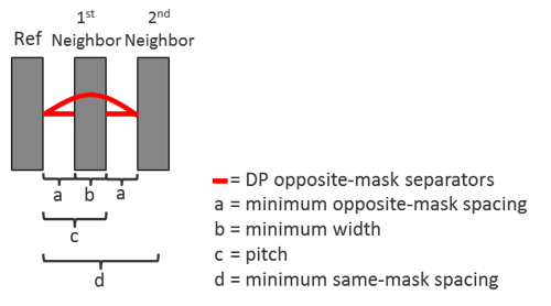
As the requirements for double patterning (DP) in integrated circuit (IC) designs become more complex with each new process technology node, DP errors become more complex as well. Adding to the challenge, many DP errors can actually cause secondary DP errors. Debugging all of these DP errors is highly inefficient, and uses unnecessary designer time. The Calibre Multi-Patterning tool intelligently filters out complex DP errors and partitions them into targeted categories. This filtering helps designers identify and eliminate the root cause of DP errors that, when resolved, also eliminate all related errors generated as a side effect. This expanded filtering, combined with enhanced visualization, enables design teams to improve error debug efficiency in all types of DP configurations. Through these novel detection and visualization algorithms, the Calibre Multi-Patterning toolset has evolved to meet the increased complexity of advanced node DP verification.