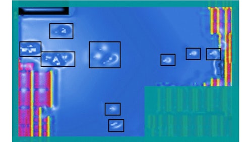
Design teams set power, performance, and area (PPA) targets for their IC designs that reflect the product’s intended market and uses. During physical implementation, they strive to create a layout that satisfies these targets. Google encountered voltage (IR) drop issues during the development of a 5 nm design. Attempting to resolve these impacts using place and route (P&R) solutions coupled with manual adjustments was extremely time-consuming, requiring multiple iterations and significant engineer resources. They needed a solution that would enable fast, accurate, and efficient layout optimization for the reduction of IR drop violations during design implementation. The Calibre DesignEnhancer solution from Siemens EDA provided Google with a push-button solution that enabled the design team to significantly reduce IR drop in their design without impacting performance or area targets, enabling them to complete design implementation quickly and efficiently while ensuring the design satisfied its power management target.
Automated DRC-clean layout optimization during IC design implementation reduces IR drop for fast, effective power management
Google was looking for a fast and easy way to reduce IR drop violations by applying DRC-clean layout enhancements to their design during the design implementation stage. They turned to the Calibre DesignEnhancer tool from Siemens EDA, an automated, analysis-based layout optimization solution designed to be used in conjunction with P&R tools and flows. The Calibre DesignEnhancer tool provides multiple layout enhancement technologies that help reduce IR drop without negatively impacting performance and area. The user-friendly push-button operation requires minimal training and setup, and because the Calibre DesignEnhancer software relies on Calibre engines and Calibre rule decks, all layout modifications are correct by construction and DRC-clean.
Products
Calibre
Industry Sector
Semiconductor devices
Electronics
