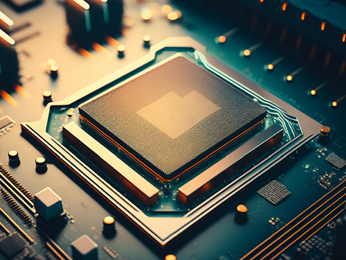
Ensuring 3D IC Semiconductor Reliability: Challenges and Solutions for Successful Integration
Understanding the Benefits of 3D IC Semiconductor Design
There are significant benefits to 3D IC and chiplet-based design
3D IC enables companies to partition a semiconductor design and integrate silicon IP at the most appropriate process node and process, providing low latency, high-bandwidth data movement, lower manufacturing costs, higher wafer yields, lower power consumption and overall lower costs.
Challenges in Ensuring 3D IC Semiconductor Reliability
3D IC integration requires ensuring the reliability of new components
These include:
Through-silicon vias (TSV) that connect the front and backside metal stack in the active dies or passive interposers to allow for vertical die stacking
Through-compound vias that can connect chiplets vertically through oxide or organic material for large distances
Micro bumps for the vertical connection of chiplets at close range
Copper pads for hybrid bonding and redistribution layers to connect various 3D IC chips.
Solutions for Reliable 3D IC Semiconductor Design and Integration
Download this eBook as we explore some of the challenges 3D IC assemblies impose when ensuring manufacturability and reliability.