Nokia uses Xpedition portfolio to increase design process efficiency
Enhancing physical design reuse within PCB flow
Nokia
As a trusted partner for critical networks, Nokia is committed to innovation and technology leadership across mobile, fixed and cloud networks.
https://www.nokia.com/- Headquarters:
- Helsinki, Finland
- Products:
- Xpedition Enterprise
Using Xpedition, we were able to successfully shorten design time while maintaining uncompromised quality.
Nokia
Implementing Xpedition was the right choice for us.
Nokia
Technology leader motivated to improve processes
Nokia is a global technology company that operates in over 130 countries and recorded net sales north of $22 billion in 2021. Nokia delivers critical networks through technology leadership and trusted partnerships to help meet some of the most pressing challenges the world faces, such as climate change, the digital divide, and stalling productivity growth.
Nokia combines radio research, development, and manufacturing under the same roof in a unique way at its Oulu, Finland site, also referred to as “home of radio.” It is in fact is one of the leading radio research hot spots in the world. The site benefits from the surrounding industry ecosystem and actively cooperates with the University of Oulu in 5G and 6G research.
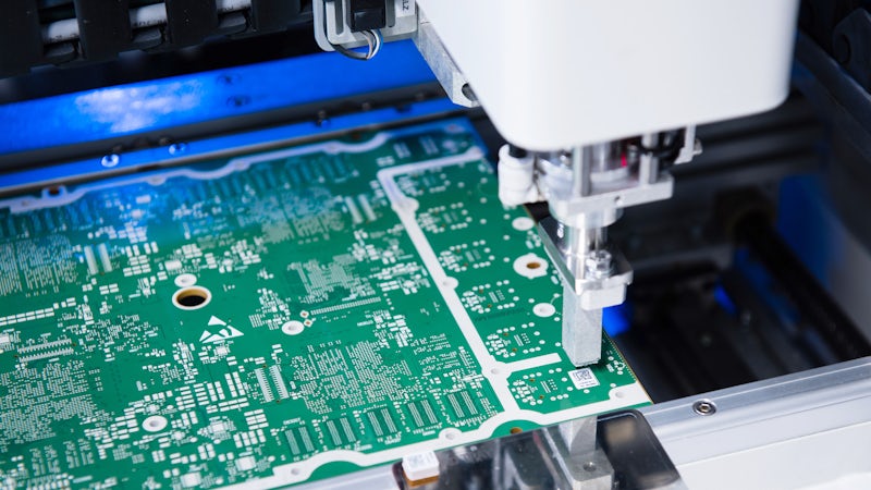
At its Oulu site, Nokia designs entire radio systems. Nokia’s products can consist of multi-board systems, and one board can consist of over 15,000 components. The company is constantly looking for ways to further improve its design processes in this complex environment.
One of the more complex challenges Nokia faced was integrating different functionality and a variety of technologies (digital, RF, analog-mixed signal) on single board products having very small form factors.
-640x360.jpg?w=900&fit=max&q=60&dpr=1&auto=format)
Nokia Oulu, Finland
Finding the right solution
Nokia’s workflow spans multiple teams and multiple domains, heightening the importance of concurrent engineering and collaboration among several design disciplines, all the way from design to manufacturing.
Nokia wanted to make its design flow faster and physical design reuse more efficient, so it turned to Siemens EDA, with whom it was already a customer. Based on identified requirements, Siemens EDA added new methodologies to its Xpedition™ Enterprise software.
With Xpedition, Nokia’s electronics engineering teams could better leverage concurrent engineering and the reuse of existing designs in new products through optimized component management. Xpedition also helped improve process automation and the accuracy and speed of design verification.
Implementing Xpedition was the right choice for us,” said Markus Välkky, Squad Group Lead, PCB Technology at Nokia. “Using Xpedition, we were able to successfully shorten design time while maintaining uncompromised quality.”
-640x360.jpg?w=900&fit=max&q=60&dpr=1&auto=format)
Markus Välkky, Squad Group Lead, PCB
The benefits of physical design reuse
The reuse of circuit board physical designs has not been very widely utilized in the industry; however, it is now gaining popularity because it enables design teams to realize significant time savings and lower development costs. At Nokia, product quality and time-to-market are imperative to success.
“Quality is first for us, then time-to-market and cost,” said Ari Oinas, Technical Leader, PCB Design at Nokia.
The advantages of Nokia’s Xpedition reuse flow are particularly relevant to board simulations. Naturally, everything must be simulated on the board to ensure operability, including the reused physical design, the schematic, and the physical layout. However, as Nokia builds very complex, high density boards, simulating an entire design is almost impossible. This is exacerbated by the variety of on-board technologies and the different effects that must be simulated, including RF, EMC, EMI, and thermal.
“If we take the antenna array case, you create the first draft of this small block,” said Oinas. "Then you send it over multiple times to simulation and get changes back. There are frequent changes to that single block instance. There is also a lot of routing between blocks, which makes the process time-consuming.”
The breakthrough came when Nokia adopted Xpedition and its extended support of physical design reuse. Now, once the engineering team verifies a block instance, they can reuse it as known-good physical IP that they do not have to simulate again. This saves a significant amount of time and effort because when a change to a block is required, the entire block does not have to be recreated, only the single affected instance is replaced. Overall simulation time is reduced because they can reuse this pre-verified physical IP.
With the Xpedition reuse flow, once an instance is completed and verified, its fidelity is maintained as a single source of truth. Xpedition ensures that a finished piece of reusable physical IP is locked and cannot be changed. Every member of the team — regardless of domain or discipline — is confident that they can rely on the specific reusable blocks. Engineers can simply place those proven instances where they want them and know they will work. They can also move instances later, if needed, without introducing errors.
Management of physical components clearly benefitted from this new approach. Before adopting Xpedition, it took more time to trace back errors and alterations in the design or implementation, especially when multiple layout designers were working on the same board.
“Before transitioning to the physical reuse approach, design alterations and repetitive tasks increased the possibility of error,” said Oinas. “This led to processes that were not optimal.”
-640x360.jpg?w=900&fit=max&q=60&dpr=1&auto=format)
Ari Oinas, Technical Leader, PCB Design
A faster path to market-leading, high-quality 5G designs
Although the size of a particular circuit and the degree to which it uses previously implemented schematics determine how much time can be saved during the design process, in general, Xpedition helped Nokia achieve its target in improving design productivity.
“Siemens provided great collaboration,” said Oinas. “This was a pretty significant productivity impact as our development cycle was shortened using Xpedition. At the same time, we were able to have consistent quality in each channel. Given the complexity of our board designs, we are very pleased with the results.”
Due to this success, Nokia plans to deploy the Xpedition-based reuse methodology across other advanced designs. Already, Xpedition, is part of the Siemens Xcelerator business platform, is helping Nokia realize tomorrow’s 5G designs today.
Siemens provided great collaboration.
Nokia
Given the complexity of our board designs, we are very pleased with the results.
Nokia